
Fabless to Fearless: India's Path to Semiconductor Competitiveness
Introduction: India is Building Chips to Power its Digital Day
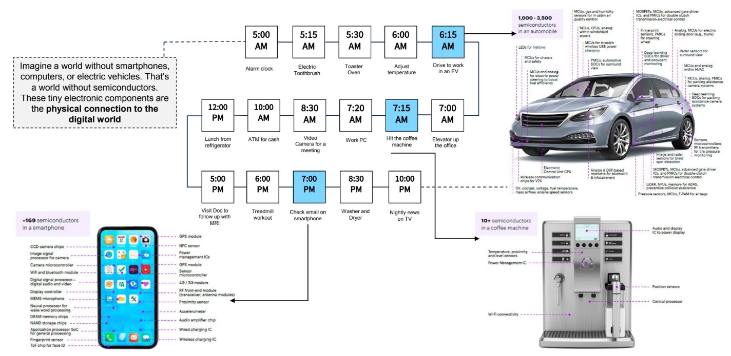
Semiconductors are no longer just components, they are infrastructure. As essential to the 21st century as steel, oil, or electricity were to the last. Every industrial value chain, from AI and aerospace to energy, and healthcare, now rests on a layer of silicon. A modern smartphone contains 100 to 150+ semiconductor components. An EV can contain 1,000 to 3,000+ chips, depending on autonomy and electronics content.
Caption: From waking up to driving, working, and winding down → semiconductors power nearly every object we interact with. A modern smartphone contains 100–150+ semiconductor components; An EV can contain 1,000–3,000+ chips, depending on autonomy and electronics content. Even your morning coffee machine has 10+. (Source: Accenture)
The post-COVID world has made this abundantly clear. Supply chain disruptions exposed our dependency on a fragile, hyper-concentrated manufacturing base. Car factories shuttered for months. Tech giants scrambled for data center system allocations. Even washing machine manufacturers faced production delays. The world learned a hard lesson: semiconductors are critical infrastructure, and countries without access to them cannot build the products their economies depend on. AI's explosion has further strained global GPU supply, while geopolitical flashpoints from the Taiwan Strait to the US-China tech cold war have transformed chips into instruments of statecraft.
In response to repeated supply-chain shocks and rising geopolitical risk, governments worldwide are ramping up industrial policy to rebuild semiconductor resilience. The US CHIPS and Science Act authorises $52.7 billion in incentives for domestic manufacturing, R&D, and workforce development. The EU Chips Act aims to mobilise tens of billions of euros in public-private investment to strengthen Europe's semiconductor ecosystem. China's National Integrated Circuit Industry Investment Fund has accumulated $95 billion to support domestic chip capacity, while Japan is backing its semiconductor revival through subsidies and tax incentives including support for Rapidus.
India is moving decisively to be part of this shift:
- The Tata Electronics and PSMC Fab in Dholera, Gujarat will target 50,000 wafers per month. This project represents India's first large-scale commercial semiconductor manufacturing facility, with an investment of ₹91,000 crore (approximately $10.9 billion), expected to begin production by December 2026, focusing on 28nm compute and power management chips.
- The Tata Semiconductor Assembly and Test (TSAT) ATMP Unit in Assam will be India's first indigenous semiconductor assembly and testing facility. With an investment of ₹27,000 crore ($3.3B), it will target a daily output capacity of 48 million chips.
- CG Power and Industrial Solutions OSAT Facility (Sanand, Gujarat), in partnership with Renesas Electronics and Stars Microelectronics, is being set up with an investment of ₹7,600 crore, focusing on legacy packages and advanced solutions for automotive, consumer electronics, and industrial applications.
- The HCL Foxconn Joint Venture (Jewar, Uttar Pradesh), approved in May 2025, will manufacture display driver chips with an investment of ₹3,700 crore and a capacity of 20,000 wafers per month.
- Kaynes Semicon OSAT Unit (Sanand, Gujarat), approved in September 2024 with an investment of ₹3,307 crore, will have a capacity of 6.3 million chips per day, catering to automotive, industrial, and consumer electronics.
- Micron Technology's OSAT Facility (Sanand, Gujarat), approved in June 2023, focuses on assembling and testing DRAM and NAND products for domestic and international markets, with Phase 1 expected to begin operations in 2025.
- The IndiaAI Mission, approved by Cabinet in March 2024 with ₹10,300+ crore allocation over five years, is building a facility with 18,693 GPUs, one of the world's most extensive government-led AI compute infrastructures, with direct semiconductor linkage through AI-optimised chip requirements.
- The Research, Development and Innovation (RDI) Scheme (₹1 Lakh Crore), approved by Cabinet in July 2025, is the largest private sector R&D incentive scheme in Indian history, with dedicated funding for semiconductors, quantum computing, AI, and deep technologies, 50% financing available for transformative semiconductor projects at Technology Readiness Levels 4 and above, and a Deep-Tech Fund of Funds to support semiconductor startups.
- In 2023, India signed a semiconductor supply chain MOU with the US under the iCET framework, laying the groundwork for long-term ecosystem development, talent alignment, and supply chain cooperation.
These efforts signal that India is intent on entering the semiconductor map as a future manufacturing and packaging node, not only as a design hub. India's entry into semiconductors is about identifying high-leverage, capital-efficient wedges and building where design strength, trusted geopolitics, and domestic demand converge. This decade is India's chance to shape how the next trillion dollars of semiconductor value will be built, packaged, and deployed.
Market Overview: Why This Industry Matters
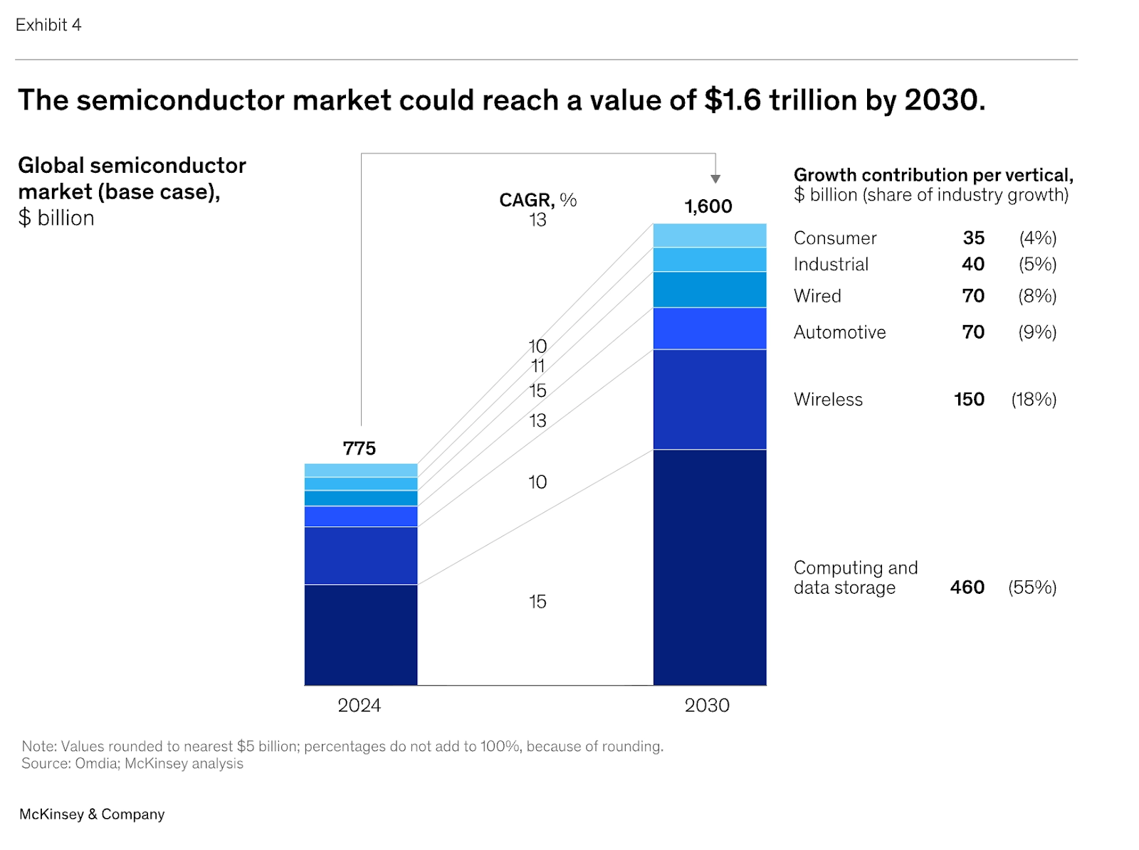
The global semiconductor market is expanding to become the backbone of modern economic, technological, and geopolitical power. By 2030, semiconductors are expected to surpass the GDP of most countries, becoming a $1 trillion industry. Their impact is nonlinear: for every $1 spent on semiconductor output in the US, $1.32 is generated elsewhere in the economy, and in a fast-growing economy like India, the multiplier could be even greater.
India is the world's fastest-growing electronics market, yet it imports over $15.6B of semiconductors annually, a figure that doubled in just one year and is still rising. This creates both urgency and opportunity: to localise critical parts of the chip value chain, whether in fabless design, specialised packaging, or domain-specific silicon for AI, automotive, and connectivity. India is already a design superpower, contributing 20% of the global chip design workforce, with engineers working on every major chip being taped out today. The goal now is to translate this design strength into downstream leverage, building high-value layers in advanced packaging, analog and mixed-signal IP, verification, and trusted chip manufacturing.
India's semiconductor opportunity must also be viewed in the context of its broader economic ascent. The country is projected to become a $7 trillion economy by 2030 and $32 trillion by 2047, with the world's second-largest and youngest workforce. Electronics exports are expected to cross $2 trillion, and per capita income will rise from $2,600 to $22,000 over this period. This sets the stage for India to leapfrog from being the world's IT and SaaS back-office to becoming a deeptech and advanced hardware powerhouse. A stable central government, rising R&D investments, and a clear policy focus on digital infrastructure, compute, and electronics make this an increasingly achievable trajectory.
To unlock the next frontier, India must venture toward:
- Domain-Specific ASICs: As general-purpose chips hit scaling ceilings, Application-Specific Integrated Circuits with tailored architectures are becoming essential, especially for AI inference, robotics, telecom, and automotive. India's software-rich ecosystem and demand-led verticals make it well-suited to lead in domain-specific silicon, where efficiency, latency, and cost control matter more than bleeding-edge process nodes.
- Power-Optimised Compute Architectures: India will need to support both ultra-low-power chips for wearables, IoT, and embedded systems, and high-performance chips for data centres, edge AI, and national compute needs. This opens opportunities for specialised semiconductor design in power-aware architectures and hardware acceleration, using GaN (Gallium Nitride) and SiC (Silicon Carbide) for more efficient power conversion, thermal performance, and faster switching in automotive, grid, and compute applications.
- Advanced Materials: Traditional silicon is reaching physical limits. India can invest in materials innovation across substrates, interconnects, and packaging, from high-k dielectrics and low-k insulators to compound semiconductors. Research-driven partnerships with IITs, IISc, and CSIR labs can enable upstream defensibility and help India shape the post-silicon materials stack.
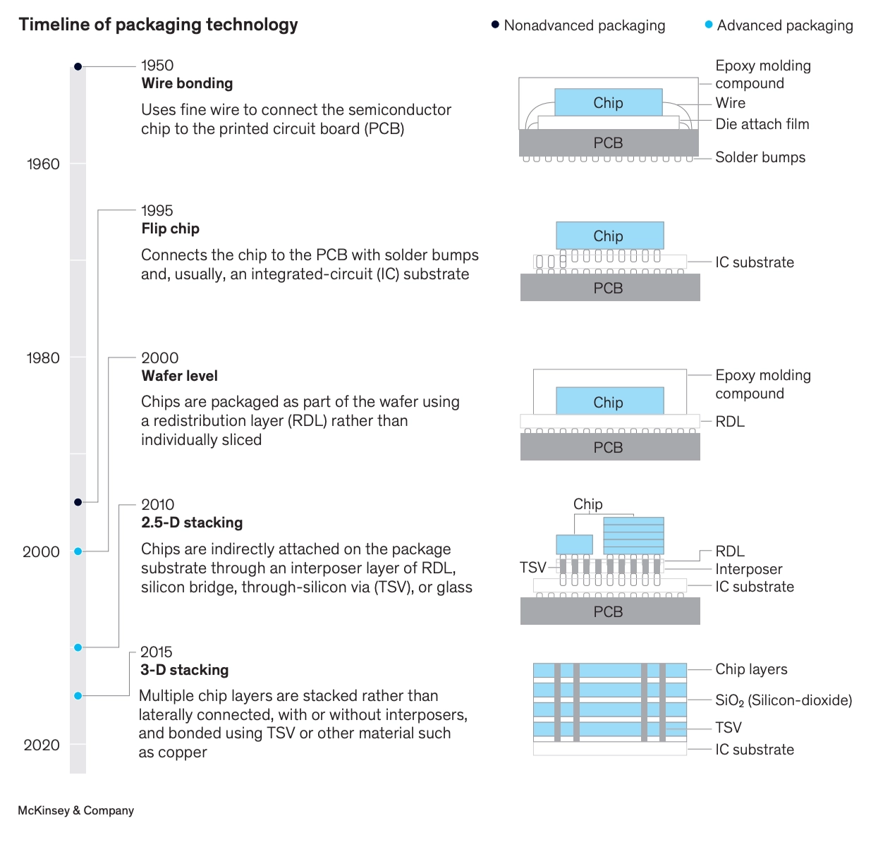
- Process Technology Alternatives: Rather than chase 2nm fabs, India can invest in non-scaling innovation including 3D integration such as chiplets and TSVs, backside power delivery, monolithic 3D ICs, and BEOL breakthroughs. These unlock density, performance, and energy efficiency without requiring cutting-edge EUV fabs, playing to India's capital-efficient advantage.
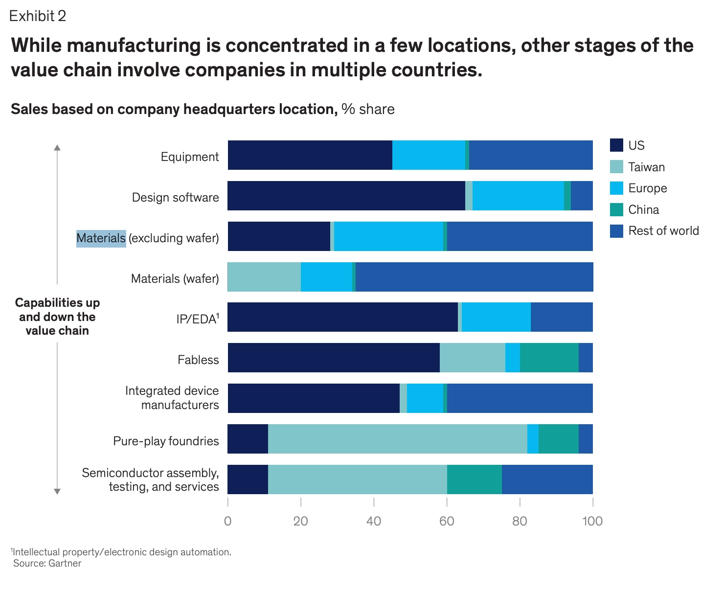
How the Value Chain Works: Where Leverage Lies
The semiconductor value chain is one of the most complex and globally distributed industrial systems ever built. It can broadly be split into three phases: Design, Fabrication, and Assembly, with some players owning specific niches and others operating as vertically integrated giants (IDMs).
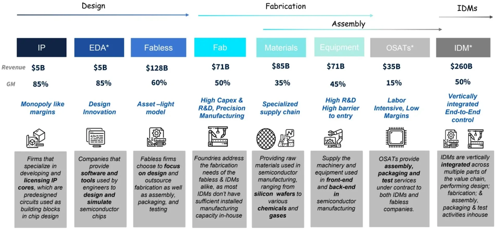
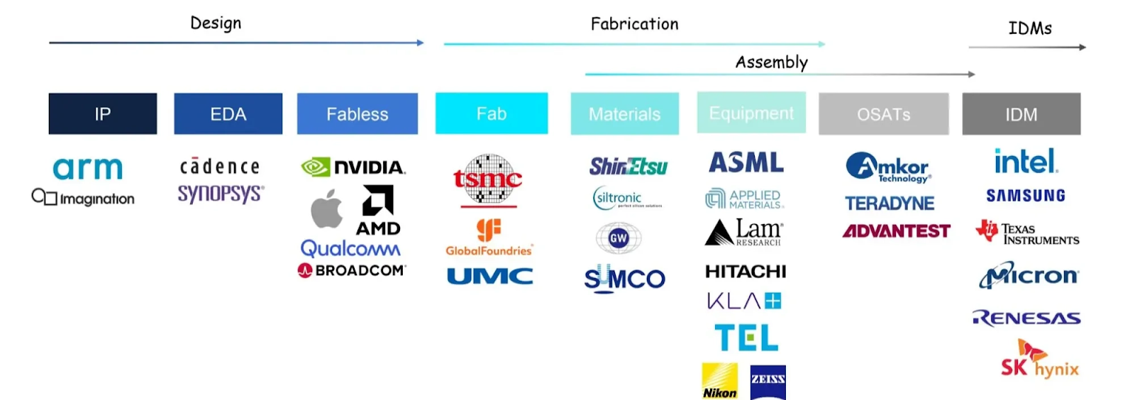
The semiconductor design process is the intellectual bedrock of chipmaking, accounting for 50% of the value in the entire value chain. It begins with licensing reusable IP cores, which are modular, pre-verified building blocks. Designers then integrate these cores to create a cohesive architecture. Using EDA tools, they simulate logical and physical behaviour, optimise floorplans, and co-optimise with foundry constraints. After verification, a test wafer is fabricated to validate manufacturability. This process is R&D-intensive, absorbing 53% of total industry R&D and 13% of capex, and can take 4 to 5 years and $500M to $1.5B at advanced nodes.
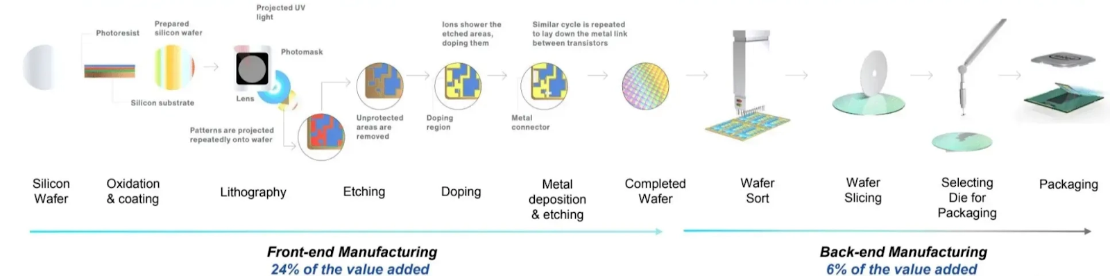
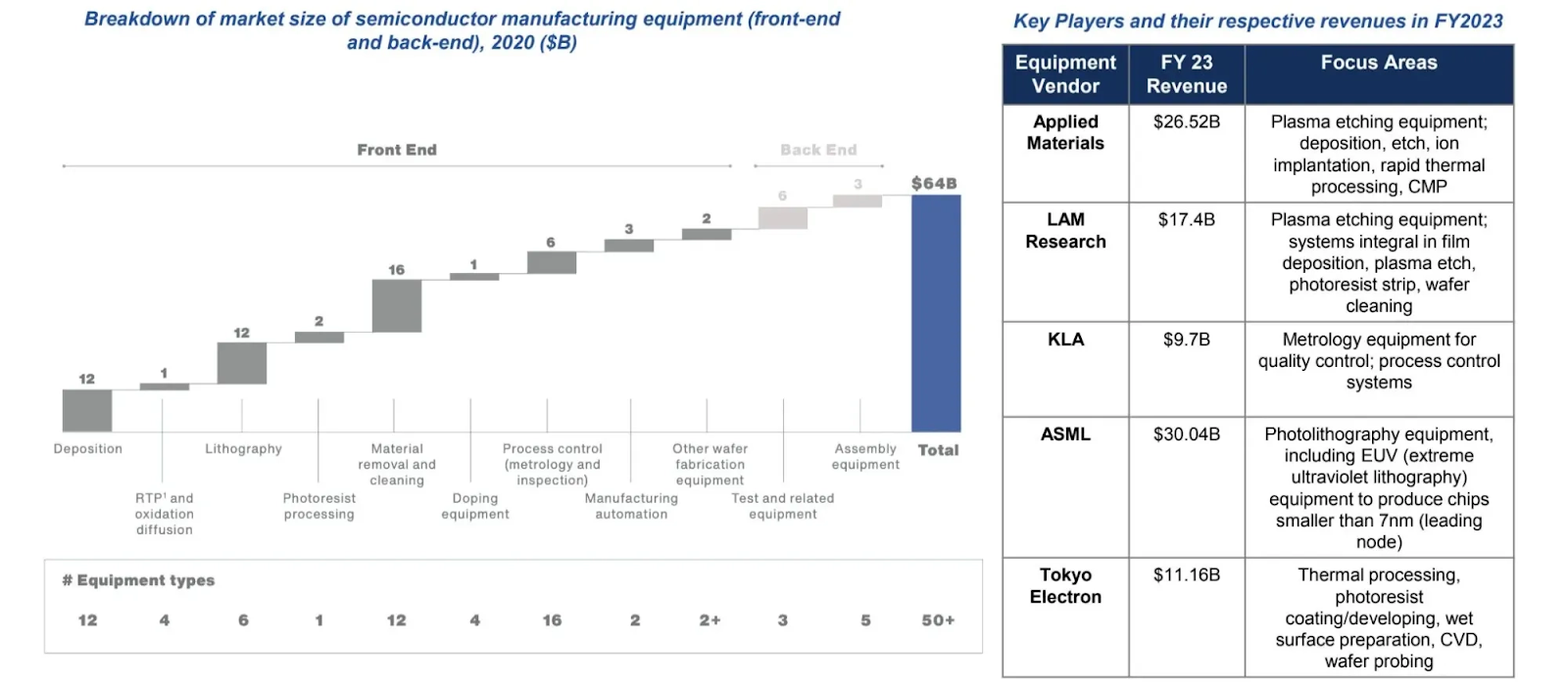
Semiconductor manufacturing dominates industry capex with 77% spent on fabrication alone. Front-end processing involves 350 to 700 steps like lithography and doping, demanding near-perfect yield over 45 to 60 days. Back-end follows with wafer slicing, probing, and advanced packaging. Despite its complexity, back-end adds just 6% of value while front-end contributes 24%, underscoring the capex-heavy but uneven value distribution across the chain.
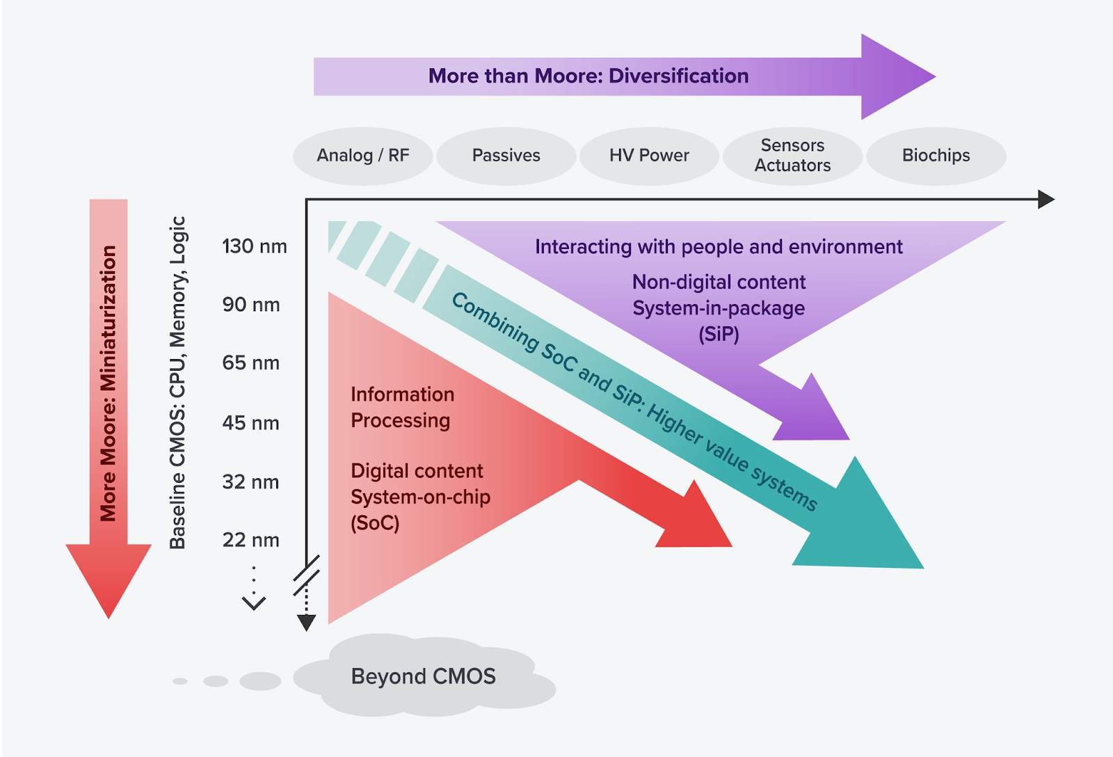
The $573B semiconductor industry is split across logic (42%), memory (26%), and analog, power, and sensor chips (32%). Logic and memory alone drive 67% of global revenues, underpinning compute-heavy domains like AI, data centres, and mobile. The industry is bifurcating: on one axis is "More Moore," the relentless push to shrink transistors for logic and memory; on the other is "More-than-Moore," where innovation lies in integrating sensors, power, RF, and analog into SiPs and full-stack modules. India's opportunity lies in mastering both, leveraging design talent for SoCs while building capability in system integration, packaging, and functional diversification.
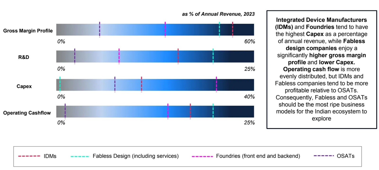
Fabless design companies deliver the highest gross margins with low capital intensity, making them the most financially attractive model for emerging ecosystems like India. IDMs and foundries demand significant capex outlays, often exceeding 30 to 40% of revenue. OSATs sit in the middle, offering moderate profitability with manageable R&D and capex. This comparative profile reinforces why India's semiconductor strategy should double down on fabless and OSAT models: they scale faster, require less capital, and align with India's talent-rich, capital-lean strengths. While IDMs have historically constituted more than 70% of the overall sales revenue of the semiconductor industry, verticalization and technology complexity have made every layer a multi-billion-dollar opportunity.
India's Semiconductor Potential
India is at a critical inflection point in the global semiconductor reconfiguration. Rather than replicating the full stack like the US or China, India's leverage lies in tuning the value chain to its comparative advantages: talent, cost efficiency, geopolitical neutrality, and capital-efficient innovation. The government's ₹76,000 crore incentive push across DLI, PLI, and SPECS has catalysed momentum spanning fabless design, packaging, materials, and test infrastructure.
India is one of the fastest-growing semiconductor markets, with demand projected to rise from $45B in 2021 (7.6% global share) to $110B by 2030 (10.8%), driven by wireless ($62B), automotive ($12B), and industrial electronics ($9B). Coupled with India's geopolitical neutrality, this positions it as a trusted node in global chip supply chains.
India's opportunity lies in a focused, fabless-first model targeting mature-node, supply-scale segments. This strategy is anchored around six levers:
- Custom silicon for AI and telecom (edge, base stations, inference ASICs)
- India-tuned IP cores (ISRO, 6G, BharatNet, domestic standards)
- Packaging and ATMP scale-up (ATMP as beachhead, with roadmap to advanced packaging)
- Analog, power, and RF chips (industrial, EVs, power converters)
- Secure chips (digital identity, sovereign compute)
- AI-enabled EDA and Tooling: India-native platforms for verification, test automation, and ML-accelerated design workflows including RTL-to-layout, yield prediction, and analog simulation
These align with India's strengths in software and frugal engineering while enabling strategic autonomy and long-term value capture.
India's semiconductor ecosystem now touches every part of the value chain, from IP and fabless design to equipment, OSATs, and emerging IDMs:
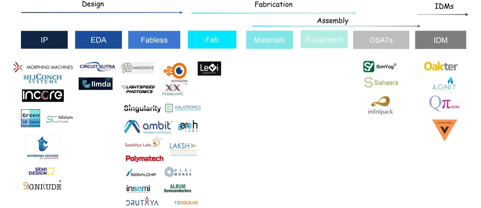
- Design and Verification (IP, EDA, Fabless): India's strongest pillar, with 20+ startups building silicon IPs, domain-specific accelerators, and verticalized logic cores.
- Manufacturing (Fab, Materials, Equipment): Early activity in specialty fabs, high-frequency packaging, and localised materials.
- Assembly (OSATs, IDM): First few IDMs are emerging with full-stack ambitions.
The current startup landscape is heavily skewed toward fabless design, with over 40 startups operating in this space. Yet early signs of diversification are visible:
- IP and EDA/AI tooling (9 startups): A nascent but crucial layer, enabling sovereign design capabilities and verification infrastructure.
- Materials (1 startup): India's chemical base presents an opportunity to localise chip-grade materials with the right refining capacity.
- IDMs and ATMP (8 startups): Full-stack efforts are emerging, particularly in analog, secure, and industrial chips.
- Fabs (1 commercial effort): Early traction in legacy-node fabs at 28nm and above, with government support.
India's startup momentum is still concentrated at the design layer, but the full stack is now in motion, with significant whitespace in tooling, materials, and advanced packaging still open for new entrants. Fabless offers high margins and low capex, ideal for India's capital-light innovation ecosystem. Foundries and IDMs are capex-heavy but strategically necessary. OSATs offer manufacturing jobs and process know-how with lower barriers. This underscores India's opportunity to build fabless scale, selectively invest in high-value OSAT capabilities, and support niche specialty fabs for analog, and compound semiconductors. India's best wedge is the "More-than-Moore" segment, power, analog, and sensors, which are large, defensible, and aligned with India's manufacturing scale-up in EVs, grid, and industrial automation.
Not all parts of the semiconductor stack are viable for India in the next decade. Display fabs are dominated by South Korea, China, and Taiwan with strong scale advantages and falling margins. Sub-28nm foundries demand over $15B per site, deep EUV IP, and strong EDA and foundry co-optimisation. DRAM and NAND markets are consolidated among three to four global players with enormous capex and volatile pricing cycles. India should prioritise fabless design, OSATs, and mature-node foundries, the verticals that maximise leverage on talent, capital, and time.
Materials and Chemicals: The Hidden Layer in Fabrication
Wafer fabrication depends on over 500 specialised process chemicals, spanning wet etchants, CMP slurries, sputtering targets, and high-purity gases. As nodes shrink and EUV becomes standard, the volume and complexity of these materials continue to rise, with advanced fabs now requiring ultra-pure hafnium, ruthenium, GaN, and graphene-based compounds. In 2019 alone, front-end materials accounted for $33B, led by silicon wafers (36%) and photoresist chemicals (16%), while back-end materials totalled $19B, dominated by organic substrates and leadframes.
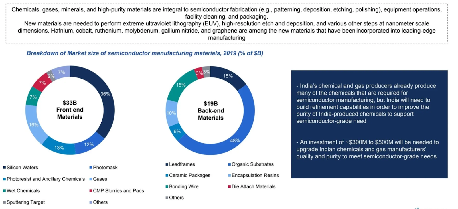
India's chemical industry already produces many of these base inputs but lacks the refinement capacity and purity control required for semiconductor-grade use. This presents a high-leverage opportunity: with $300 to $500M in targeted investment, India could upgrade its purification infrastructure and become a reliable source of critical materials in a geopolitically fragile supply chain. India can also play a critical role in localising input dependencies across specialty gases, etchants, and slurries for fabs, and vacuum components, inspection tools, and power delivery subsystems. This upstream layer is consistently overlooked but essential for resilience.
Where We Are Today: Challenges and Entry Points
India holds 20% of global design talent with 125,000 or more engineers, delivering 3,000 chip designs annually and contributing 50% of global design value-add. Yet fabless startups remain undercapitalised, with limited access to MPWs and prototyping fabs, prohibitive EDA and IP licensing costs, and total ecosystem revenue under $50M per year. Startups are often stuck in low-margin, high-volume verticals like IoT, energy meters, and MCUs. A step-function change in risk capital and accessible prototyping infrastructure is required to scale.
India imports 90% of its semiconductor consumption, including critical components for telecom. While policy aims to raise local sourcing to 17% by 2026, upstream material inputs remain a blind spot. Wafer fabrication relies on ultra-pure specialty chemicals and high-purity process gases, and targeted investments in refinement infrastructure could establish India as a critical materials exporter in a fragile global supply chain.
India is investing in Assembly, Testing, and Packaging, which is labour-intensive and volume-driven, matching India's workforce advantage. While five ATP facilities are plausible near term, advanced packaging in 2.5D and 3D will soon dominate, and labour arbitrage will fade. Global integration with design and foundry partners will be key to staying competitive. India's proposed fabs at 28nm and above target automotive, IoT, and industrial chips and can anchor viable supply chains when tied closely to local demand, packaging, and fabless activity.
India has 40+ chip startups, but revenue remains under $50M per year, prototype and test infrastructure is scarce, and VC risk appetite is nascent. There is strong technology and intent, led by former MNC executives and top academic PIs, backed by schemes like DLI, C2S, iDEX, and TTDF. There is potential to leapfrog in areas like custom ASICs, power electronics, and 6G hardware stacks, especially if tied to domestic missions across ISRO, DPI, and BharatNet.
India's positioning is underpinned by five comparative strengths. India's design talent enables end-to-end chip development and is a natural platform for fabless scale and design-led partnerships. Few countries offer the scale of domestic pilots for silicon validation that India does through EVs, Aadhaar, UPI, and BharatNet. India's 50% lower R&D cost base allows chip development at seed-stage capital levels, ideal for fabless entrepreneurship. India is one of few nations trusted across the US, EU, Japan, and the Global South, enabling secure co-design, sovereign compute, and de-risked supply chains. And few emerging economies have dedicated this level of state focus, with India's support stack spanning DLI reimbursements, SPECS and PLI infrastructure grants, R&D grants through iDEX, C2S, and TTDF, and academic MoUs with IITs, IISc, and global labs.
India's long-term edge in semiconductors will come from building on these differentiated strengths: an abundance of design talent, trusted geopolitical neutrality, rising domestic demand, and a growing base of startups targeting under-penetrated value chain segments. The real leverage lies in owning design IP, OSAT throughput, and front-end innovation across India-tuned chiplets, secure embedded silicon, high-yield analog and power ICs, and localised packaging.
What the Indian Ecosystem Needs
To turn momentum into market outcomes, India must close key systemic gaps:
- Government Grants for R&D: Schemes like DLI, iDEX, and TTDF have laid the foundation but need deeper alignment with startup timelines, milestone-based disbursement, and continuity beyond initial prototyping. A predictable, well-capitalised R&D stack is critical to support risk-taking at the design and tooling layers.
- Anchor Customers for Early Validation: Government entities like DRDO, NTRO, ISRO, and MeitY must adopt Indian chips as strategic convictions, not policy mandates. These become the proving grounds that derisk scale-up for commercial buyers.
- University-Startup Bridges: Academic programs like C2S are a good start but need tighter integration between Tier 1 institutions and early-stage ventures. Labs must prototype, partner, and push toward product, not stop at publication.
- Policy and Bureaucratic Reform: Workflows from fab floors to ports and airports are still inundated with bureaucratic delays. Customs regulations insert weeks and months of delay into shipments of critical equipment in and out of the country. Labour codes are not designed to allow 24-hour cycle times on fab and factory floors. Common-sense deregulation and reform will help accelerate Indian competitiveness.
- Global Business Development: India's neutrality is an asset. India can export secure, affordable chips to underserved and geopolitically cautious markets from Southeast Asia to Africa and Latin America, where supply chain diversification is an active priority.
- Venture Capital That Underwrites Deep Tech: India needs investors who back IP-heavy companies with long gestation and nonlinear upside. The semiconductor curve looks different from SaaS, and requires patience, domain depth, and conviction in long-term compounding.
Our Thesis in Action
At 3one4 Capital, we have always believed that India's semiconductor opportunity would start with bold founders solving hard problems from first principles. The proof is already here.
Agnit Semiconductors: Powering the Future with GaN Innovation
Born from cutting-edge research at IISc Bangalore, Agnit Semiconductors is pioneering Gallium Nitride (GaN) power devices in India. GaN offers higher efficiency, faster switching, and reduced energy loss compared to traditional silicon-based power electronics, making it the preferred material for EVs, solar inverters, fast chargers, aerospace, and data centres. GaN is a wedge where India can build a position in a material transition that legacy supply chains have not yet locked down. Agnit is building from day one to global specifications while tapping local demand across power-critical sectors. By investing early, we have backed a company at the forefront of the transition to wide-bandgap semiconductors, with IP defensibility and strong adjacency across energy, industrials, and mobility.
H2LooP: AI Infrastructure for Embedded and Automotive Systems
Software complexity in embedded systems is rising exponentially, crossing 100M+ lines of code, governed by strict standards like MISRA and ASPICE, and fragmented across HALs, BSPs, and safety documentation. Today's engineers rely on disconnected stacks of static analysers, linters, and tribal knowledge. H2LooP is solving this with domain-specific small language models tailored for system engineers. The platform acts as a co-pilot for debugging, documentation, compliance, crash log analysis, and low-level code mapping. Built on India's deep embedded talent pool, the company is already landing pilots with Tier 1 OEMs and scaling via cloud partnerships. The next compute layer is the AI that helps engineers build and debug atop silicon. H2LooP demonstrates how India can lead in vertical AI infrastructure, with teams that understand both low-level systems and modern ML and are building the co-pilots for the world's most complex, regulated codebases.
Scimplify: Materials-as-a-Service for the New Supply Chain
Scimplify is building a digital-first platform for the sourcing, development, and manufacturing of specialty chemicals, serving pharma, agro, personal care, and advanced materials customers. With over 30 partner plants and an R&D hub in Genome Valley, they enable rapid, made-to-order production of high-margin specialty chemicals for both domestic and export markets. Upstream leverage in semiconductors comes from localising materials: etchants, slurries, precursors, and gases. Scimplify's orchestration layer helps derisk that dependency while tapping India's $220B chemical base. Their AI-powered manufacturing stack (ATOMS) is already deployed across 500+ customers, ensuring compliance with global standards including GMP, CGMP, and FDA requirements. It is a scalable wedge into the overlooked but essential materials layer of advanced manufacturing.
The Call to Build
The next wave of semiconductor innovation will be shaped by countries that bring trust, cost efficiency, and differentiated talent to the table, and India has a genuine and distinctive position across all three. India's design depth, its geopolitical neutrality in a fractured world, its sovereign demand across digital infrastructure, and industrial automation, and its growing base of IP-led startups give it a set of starting conditions that no other emerging economy can replicate at this moment. The government has committed capital at scale, the policy stack is in place, and a first generation of founders is already proving that India can build at the frontier of semiconductors, materials, and embedded AI. What this decade demands is that venture capital, anchor institutions, and the ecosystem move with the urgency the window requires, backing founders on semiconductor timelines and treating India's cost constraints and demand characteristics as the design brief for globally competitive products. For founders building at the intersection of silicon, software, and systems, the opportunity is structural and the foundation is here.
DISCLAIMER
The views expressed herein are those of the author as of the publication date and are subject to change without notice. Neither the author nor any of the entities under the 3one4 Capital Group have any obligation to update the content. This publications are for informational and educational purposes only and should not be construed as providing any advisory service (including financial, regulatory, or legal). It does not constitute an offer to sell or a solicitation to buy any securities or related financial instruments in any jurisdiction. Readers should perform their own due diligence and consult with relevant advisors before taking any decisions. Any reliance on the information herein is at the reader's own risk, and 3one4 Capital Group assumes no liability for any such reliance.Certain information is based on third-party sources believed to be reliable, but neither the author nor 3one4 Capital Group guarantees its accuracy, recency or completeness. There has been no independent verification of such information or the assumptions on which such information is based, unless expressly mentioned otherwise. References to specific companies, securities, or investment strategies are not endorsements. Unauthorized reproduction, distribution, or use of this document, in whole or in part, is prohibited without prior written consent from the author and/or the 3one4 Capital Group.
.jpg)

-p-500.webp)
.jpg)


